There comes a time in the life of every electronic hobbyist when building circuits on stripboard (aka Veroboard) is just not enough.
For those who aren’t into electronics, some background: stripboard is a sheet of fiberglass, with rows of copper tracks along it. The tracks have holes in. To make a circuit, you solder the components into the holes, make breaks in the tracks where you don’t want a connection, and cut and solder short jumper wires where you do.
Stripboard – starts out as useful and helpful, then turns on you like a rabid dog.
It’s fine for simple projects … but it becomes a pain very quickly, for all sorts of reasons. Soldering it tends to look ugly (hot solder has a tendency to fill the surface it touches, so it flows down the tracks rather than just staying in a little blob). Sometimes the solder will bridge across tracks, and can be hard to see – so you can spend a long time looking for faults in your circuit design which actually don’t exist.
The distance between the holes is not always compatible with some of the components you might want to use (usually exotic connectors), and certain types of circuits (such as higher-spec video circuits) tend to suffer poor quality.
For the hobbyist, the solution to this is to design and ‘etch’ your own circuit layout. This involves designing the layout on computer, laser-printing it (several times) onto acetate, carefully laying all the acetates on top of each other and then using them as a template to blast ultra-violet light at some special ‘photo-sensitive’ board, baking the whole thing in some nasty chemicals in order to burn off the unwanted metal, then clean it, then drill it. Normally, you then discover you made some schoolboy error (like laying the template incorrectly at the beginning of the process) and you’ve wasted an entire morning. But hey – that’s the nature of the hobby and I’m not sure there will ever be enough tools or clever software to prevent all cases of idiocy!
Making your own boards is a sort of rite-of-passage for people into electronics. I have postponed making my own boards for far too long. It’s not like any part of the process is particularly hard – but it requires a fair amount of initial expenditure, storage of some nasty chemicals, space to work, a patient spouse, and some investment of time to experiment. So thus far, I’ve kept to stripboard.
But some of the projects I want to do now (lots of build-my-own-computer work, and modifications to old computers and games consoles) would be prohibitively difficult to do with stripboard … so my PCB-etching time has come.
But … I have my CNC, now, don’t I? And having such a tool at my disposal makes a different etching method possible: that of separation routing (also known as isolation routing).
The notion is that rather than photo-etching your board and then burning most of the metal off, you just etch out narrow channels around the shapes you want to keep. So: you isolate each track-shaped piece of copper from the copper around it. No ultra-violet light or nasty chemicals are involved – just the removal of a very small amount of metal. It’s quick, clean, cheap and more environmentally friendly.
My CNC, though, isn’t really intended for this sort of fine work on a small area – it’s intended for cutting large pieces of wood, where accuracy isn’t quite so important. I have no idea how successful this would be. The only way to find out is to try it!
Designing the circuit
You have to begin with a design. Most people seem to use Eagle these days, or Fritzing. I’m not sure why, but I seem unable to comprehend either of those packages … which I freely admit, is stupid. I’m a bit of a luddite.
At the moment, I use an ancient (last updated in 2000) freeware package for RISC OS, called !RiscPCB. I find it very easy to use; primarily because it doesn’t do any of the posh things that other packages do. There’s no routing, no extensive library of components, no rats-nests … it’s really just an art package that lets you put tracks and pads down in a document, in a more PCB-centric manner.
For my test circuit, I’m building a composite video buffer circuit for a PAL Atari 2600 (this circuit – all credit and thanks should go to r3uk).
 A simple circuit to implement, but one for which I have a genuine need. It has a layout complex enough to highlight any errors in my algorithms or limitations in the CNC, but it is small and simple enough to do repeat experiments without getting bored or wasting a huge amount of material.
Extracting the data and creating the G-Code
!RiscPCB can export Drawfiles (which are like the SVGs of the RISC OS world) suitable for printing onto acetate. It’s not quite the ideal format I’d like, because I need the co-ordinates of the outlines of all the tracks and pads, rather than the co-ordinates of the tracks and pads themselves. But the ideal “document” format of !RiscPCB is binary, and so not easily deciphered.
My PCB-to-G-Code creation software works like this:
- Parse the drawfile and identify all the pads, tracks, holes and grooves.
- Turn those into a list
- Rebuild the circuit’s geometry by creating each pad and track as an outline, attempting to merge it with any geometry already calculated.
- “Fatten-up” each outline to compensate for the width of the drillbit (which I’m all-too familiar with, thanks to calculating all those lizards)
- Spit-out the G-Code for the CNC. One file for etching, and another for drilling.
Results
It’s probably not worth me going over the algorithm in too much detail – the most challenging part was probably the code for merging outlines together. It’s one of those things that seems simple enough … but when you start to consider all the edge cases, it quickly becomes a bit of a nightmare. A quick Googling during my research revealed it as a common problem for masters degree students to base their thesis on. Dear oh dear, that was a lot of dry reading …
Anyway … have a look at some pictures. Click on one to see it all big, like.


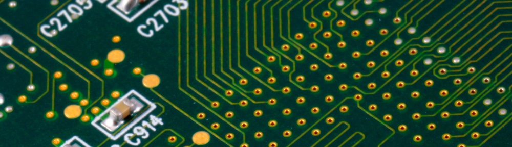
If you look carefully you can just about tell that I have approximated circles with a sixteen-sided polygon. But as that whole pad is about 3mm across, I think that’s acceptable.
The cutting was done with a special drill with a tip of only 0.3mm diameter. The blades on it are at an angle of 30 degrees, so the tracks become thicker the further down you cut.
I am really pleased with the results! I’ve included a ruler in the first picture so you can get an idea of scale. I think it’s amazing that a machine that’s supposed to cut large pieces of wood can also make such a good job of something this small and fiddly.
Yes, the holes are tiny – too tiny for component legs. That’s because they aren’t holes; they’re just engraved points (like pilot holes) for drilling with a Dremmel later. The only reason I didn’t get the CNC to drill them as a second job is because I don’t yet have a chuck that will hold the teensy drillbits!
After initial setup and preparation (which dad and I deliberately took our time over, just to make sure we got everything right) cutting that circuit took about four minutes. Estimated cost of that piece of material is about 30p. So: compared to working with stripboards or photo-etching, this method is quicker, cheaper, cleaner, safer, more environmentally friendly, more professional-looking … and makes me feel very smug, too. As things stand, I can’t see any reason for me to use stripboard, even for quick test circuits!
Next
Since I wrote all the code to do parse Drawfiles, RiscPCB’s author has suggested that I would have been better off working with the Gerber data that the software can also export. So that’s what I’m going to do next. After that, I hope I’ll be well-prepared to try double-sided boards. To do this, I’ll need to find an elegant solution to the problem of flipping the board over and aligning it perfectly before etching the second side.
I’d also like to experiment with how fine I can get the etching … reliably. My ideal goal would be to be able to place integrated circuits (where pins are 0.1 inches apart) with another track routed between them. I think I’m pretty-much there.
I’ll let you know.